%20Sdn_%20Bhd_.png)
Applications of
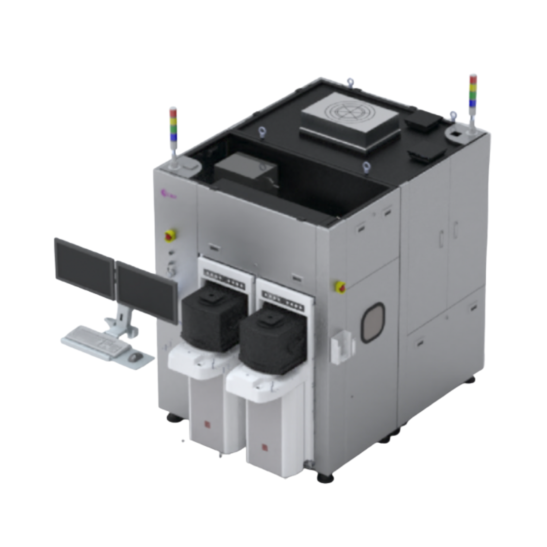
8-inch and 12-inch wafersIncoming Quality Control (IQC) for wafers, Outgoing Quality Control (OQC) for finished products
- 2.5D/3D IC
- Fan-out Wafer Level Packaging (FOWLP)
- Fan-out Panel Level Packaging (FOPLP)
Minimum detectable defect size :
1 µm
Features
- High-precision turret testing system
- Multi-light source configuration design (BF/DF)
- The fast and precise autofocus system optimizes image quality and supports complex multi-layer wafer designs.
- Super large die capability (one chip on a full 12" wafer)
- This multi-functional 2D measurement system can measure various critical dimensions
such as RDL CDs, Pad open CDs, and Bump Diameters. - The CAD Import Function is designed for ease of use and can significantly reduce recipe creation time.
- Edge detection function (EBR function) supports various wafer products (option).
Optional
- Color Filter
- High warpage wafer solutions, supporting up to ± 7mm (Option).
- Multi-Die Function Wafer Applications
- OCR SEMI standard character recognition, with a recognition rate >99%.
- Handheld Barcode Reader/RFID Function
- Specialized AI learning achieves a rule-based accuracy rate >90%.
- JDView offline verification software, which can provide Map overlay analysis.
- Recipe offline editing function
- Common Recipe Functionality (Recipe Server)
- SEMI S2/S8 Certification
- SECS/GEM Communication System
- It supports automated transport systems (OHT/AGV/MGV...).
Key defects
- RDL Damage
- Pad Open
- Short
- Residue
- Particle
- Scratch
Key Measurement
- RDL CD
- Pad Open CD
Buffalo S3002
Request for Quotation